The power of your PCB must be distributed among all its electronic components, and it is possible to lose a tiny amount of energy when sending it to the downstream components. To locate this problem and get an idea on how to rearrange the components to compensate for power losses, you can employ a large PCB Layout Design software package with a power supply analysis tool.
Once you find a problem in the simulation result, you will need to take one or more steps for PCB Board Repair. If you do this during the design phase, you can try various methods to eliminate signal integrity problems.
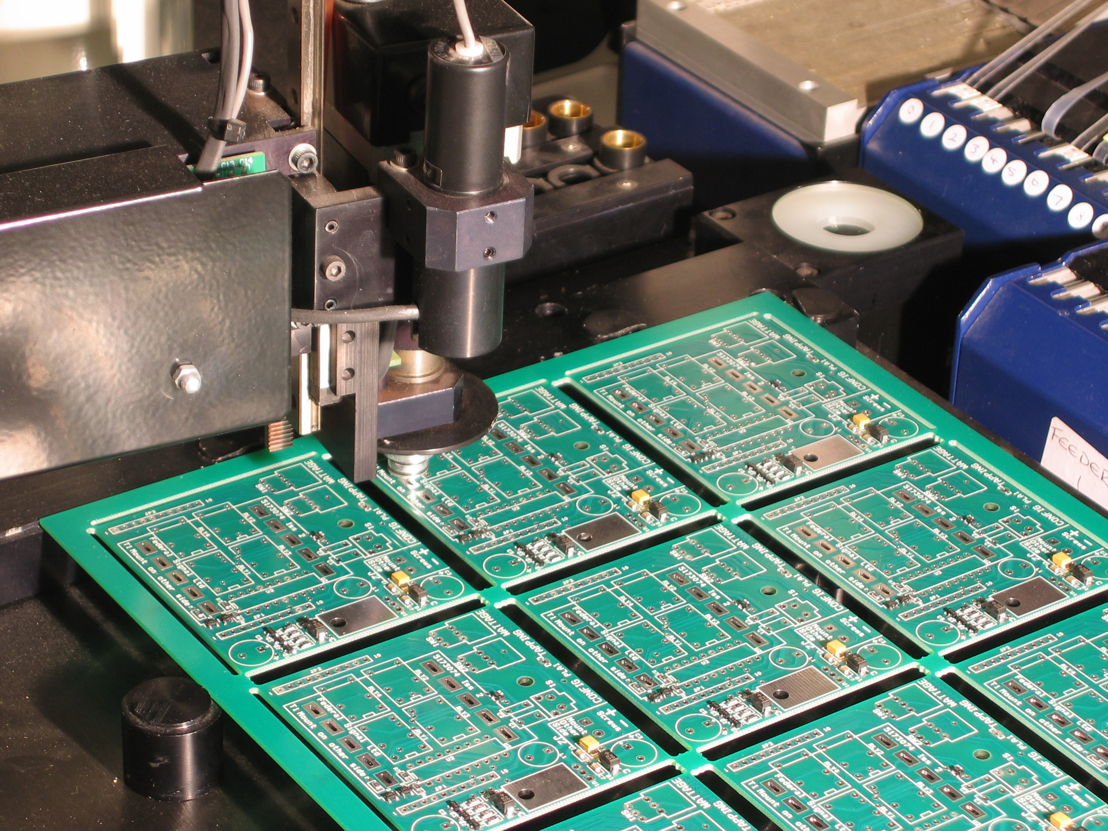
No one can rely exclusively on design rules when Fix PCB Board. Similarly, no one can rely exclusively on simulation tools to ensure that a PCB meets basic design standards. Your PCB design software should provide all of these tools in a single environment, allowing you to face any design challenge and diagnose signal and power problems during the design phase.
- To ensure that all of your PCB components are working properly, analysis of power delivery is essential. Learn more about the symptoms of a poor power supply network.
- Working with signal integrity simulations help
- Find out how you can incorporate signal integrity simulations into the design and Repair Printed Circuit Board process.
- By checking for errors using your design rules, you can ensure that your Mending PCB Board will really work the way it was designed to. You can also fix errors before going into production. Learn more about error checking using design rules.
Simulation And Verification Of Design Rules On A Unified Platform
It is very useful to work with design rules and simulation tools to avoid and solve a series of Redesign PCB Board problems that your PCB may present. The rules check features of your design should guide you through the design process, alerting you to any issues you encounter. These should always be addressed during the design phase, as it will help you for your outline and design in the proper way.
Once your design is properly formed, you can use simulations to diagnose other potential problems that cannot be quickly solved by applying the design rules. Simulations allow you to tackle more complicated issues, such as signal reflection on unfinished paths and power delivery issues due to IR drop. These two toolkits should work together, and the best way to do this is using a unified design interface.
It is extremely important to PCB troubleshooting techniques to ensure that the power, solder, and copper source of your PCB is in the right places with any surface mount technology, clearance and offset, or noise that is issued. An integrated design environment includes tools that were created to work together in a single interface. You won't have to worry about switching between multiple design interfaces with different workflows and separate functions.
Regardless of whether your circuits are going through the PCB Reverse Engineering phase after you've passed a circuit test, or you're doing a multilayer PCB, or are anticipating high noise levels, work well.